Bhd.

The four different test configuraitons are listed here: : 1. When displaying the reactive power for phase A, simply display the value in these registers with the decimal point one digit in from the right, in milli-volt-amperes-reactive. If such acts allow unauthorized access to your software or other copyrighted work, you may have a right to sue for relief under that Act. We at Microchip are committed to continuously improving the code protection features of our products. The Second Concept Most Pressed Button, MCP6V01 Thermocouple Auto-Zeroed Reference Design, PIC16F87/88. 30 MCP3909/PIC18F85J90 Single Phase Energy Meter Reference Design NOTES: DS51884A-page Microchip Technology Inc. 31 MCP3909/PIC18F85J90 SINGLE PHASE ENERGY METER REFERENCE DESIGN Chapter 4. Meter Protocol and Timings 4.1 PIC18F85J90 PROTOCOL The RS-232 port of the PIC18F85J90 is used to access the register map of the meter. REGISTER 3-13: ENERGY_VAR REGISTER Name Bit Address Cof ENERGY_VAR 64 0x100 R ENERGY_VAR_Z 64 0x108 R ENERGY_VAR_L 32 0x116 R ENERGY_VAR_L_RAW 48 0x110 R NOT IMPLEMENTED IN THIS FIRMWARE/SOFTWARE RELEASE. The gain matching registers for the standard phase need to be set to the following values when calibrating a standard phase: EQUATION 5-5: PHA_W_GAIN = 16, 384 The following equations apply for calculating the proper GLSB registers when calibrating both a standard phase, and a non-standard phase. 0000002672 00000 n
Grounds. See Figure 5-3 for meter input conditions. The numbering convention for the DS number is DSXXXXXA, where XXXXX is the document number and A is the revision level of the document. Features. 0000002326 00000 n
0000134163 00000 n
Each command ends with the ASCII character X Command Description The first byte of the data (byte 0) is an ASCII character E, L, S, W and R. E - Echo All Data Received (ECHO) L - Load Calibration Registers from Flash (LOAD) S - Store Calibration Registers (STORE) W - Write Bytes (WRITE) R - Read Bytes (READ) The last data byte is always an 'X' character. 0000003042 00000 n
PGA ADC PHA_W_OFF:32 CURRENT MCP3909 VOLTAGE ADC X CF_DEN:16 PHA_W_RAW:48 1 PHA_DELAY:8 CF_NUM:16 / Digital to Frequency Converter CF OUTPUT FREQUENCY ON PIN PHA_W:32 X PHA_W:48 PERIOD:16 PHA_W_GLSB:16 2 X X ENERGY_W_LRAW:48 ENERGY_W_Z:64 ENERGY_W:64 ENERGY_W_GLSB:16 ENERGY_W_L:64 kwh (Displayed on LCD) FIGURE 3-1: Active Energy Calculation. A4 Silicon Errata Sheet The PIC16F818/819 Rev. The ENERGY_W_L_RAW register is the register that should be read when calibrating CFNUM and CFDEN. During calibration, ENERGY_W_Z, ENERGY_W, and ENERGY_W_L_RAW will all have the same value. Dual Auto-Zeroed Operational Amplifiers. Text in angle brackets < > A key on the keyboard Press
, Courier New font: Plain Courier New Sample source code #define START Filenames autoexec.bat File paths c:\mcc18\h Keywords _asm, _endasm, static Command-line options -Opa+, -Opa- Bit values 0, 1 Constants 0xFF, A Italic Courier New A variable argument file.o, where file can be any valid filename Square brackets [ ] Optional arguments mcc18 [options] file [options] Curly brackets and pipe Choice of mutually exclusive errorlevel {0 1} character: { } arguments; an OR selection Ellipses Replaces repeated text var_name [, var_name] Represents code supplied by user void main (void) { } 2009 Microchip Technology Inc. DS51884A-page 7. Note: If number of data characters is odd, the last character (the one just prior to the 'X') will be ignored. General Description: Interfacing a MCP9700 Analog Output Temperature Sensor to a PICmicro Microcontroller. 574 0 obj
<>stream
0000003230 00000 n
C0 PIC16F506 devices that you have received conform functionally to the current Device Data Sheet (DS41268D), except for the anomalies, PIC18F2420/2520/4420/4520 Rev. Code protection does not mean that we are guaranteeing the product as unbreakable. The value is always less than one (for example, 32,767 = ) PHA_VAR_GAIN (NOT IMPLEMENTED) NOT IMPLEMENTED IN THIS FIRMWARE/SOFTWARE RELEASE PHA_VAR_GLSB (NOT IMPLEMENTED) NOT IMPLEMENTED IN THIS FIRMWARE/SOFTWARE RELEASE Microchip Technology Inc. DS51884A-page 27. 0000003385 00000 n
A2 parts you have received conform functionally to the Device Data Sheet (DS39682A), except for the anomalies, Sendyne SFP200MOD Precision Current and Voltage Measurement Module Sendyne Sensing Products Family Shunt positive (+) terminal Address selection Power & CAN communication Description The Sendyne SFP200MOD, PIC12(L)F1822/PIC16(L)F1823 Family Silicon Errata and Data Sheet Clarification The PIC12(L)F1822/PIC16(L)F1823 family devices that you have received conform functionally to the current Device Data Sheet, MCP1661 Isolated Flyback Converter Reference Design 2014 Microchip Technology Inc. DS50002313A Note the following details of the code protection feature on Microchip devices: Microchip products meet the. Ferrite beads have an impedance of the specified value at 100 MHz. 28 MCP3909/PIC18F85J90 Single Phase Energy Meter Reference Design ENERGY_W_GLSB (NOT IMPLEMENTED) REGISTER 3-18: ENERGY_W_GLSB REGISTER Name Bits Address Cof ENERGY_W_GLSB 16 0x1A0 R/W NOT IMPLEMENTED IN THIS FIRMWARE/SOFTWARE RELEASE ENERGY_VAR_GLSB (NOT IMPLEMENTED) REGISTER 3-19: ENERGY_VAR_GLSB REGISTER Name Bits Address Cof ENERGY_VAR_GLSB 16 0x1A4 R/W NOT IMPLEMENTED IN THIS FIRMWARE/SOFTWARE RELEASE CREEP_THRESH (NOT IMPLEMENTED) REGISTER 3-20: CREEP_THRESH REGISTER Name Bits Address Cof CREEP_THRESH 32 0x1A6 R/W NOT IMPLEMENTED IN THIS FIRMWARE/SOFTWARE RELEASE CF_PULSE_WIDTH CFDEN REGISTER 3-21: CF_PULSE_WIDTH REGISTER Name Bits Address Cof CF_PULSE 8 0x1AA R/W Defines CF pulse width from 0 to 255. The software allows individual configurations to be turned on or off when going through the calibration flow Microchip Technology Inc. DS51884A-page 33. The intent of the calibration process is to yield output registers that are decimal representation of the final energy, power, current or voltage value. 0000134791 00000 n
The software will read this value when performing phase to phase gain matching during active power calibration Microchip Technology Inc. DS51884A-page 29. Bit must be set for registers to begin updating, which starts on the next line cycle after bit is set. 0000133624 00000 n
499 76
trailer
Items discussed in this chapter include: Document Layout Conventions Used in this Guide Recommended Reading The Microchip Web Site Customer Support Document Revision History 2009 Microchip Technology Inc. DS51884A-page 5. A listing of sales offices and locations is included in the back of this document. Package Type. The manual layout is as follows: Chapter 1. Features. 1.2 WHAT THE MCP3909/PIC18F85J90 SINGLE PHASE ENERGY METER REFERENCE DESIGN KIT INCLUDES This MCP3909/PIC18F85J90 Single Phase Energy Meter Reference Design Kit includes: MCP3909/PIC18F85J90 Single Phase Energy Meter Reference Design, Important Information Sheet DS51884A-page Microchip Technology Inc. 11 Product Overview 1.3 GETTING STARTED To describe how to use the MCP3909/PIC18F85J90 Single Phase Energy Meter Reference Design, the following example is given using a 2-Wire 1-phase, 220V AC line voltage and connections using an energy meter calibrator equipment or other programmable load source. MCP3909. Bhd. AN1476. 18 MCP3909/PIC18F85J90 Single Phase Energy Meter Reference Design 3.2 ACTIVE ENERGY CALCULATION Active Energy is described through the process described in Figure 3-1. CONSTRUCTION OF CMOS ICs PREVENTING SCR TRIGGERING. Meter Calibration 5.1 CALIBRATION OVERVIEW The method to calculate the values for the calibration registers in Chapter 3. PIC12LF1840T39A. MCP1630 Input Boost Converter Demo Board User s Guide 2007 Microchip Technology Inc. DS51608B Note the following details of the code protection feature on Microchip devices: Microchip products meet the, Rev. endstream
endobj
500 0 obj
<. Features. The final correction factors to convert these registers to units of energy are located in the _GLSB registers. For 60 Hz line 0 to 255 * ms 0x1AB RESERVED 8 Reserved 0x1AC CFDEN 8 R/W CF Calibration Pulse correction factor 0x1AD RESERVED 8 Reserved 0x1AE CFNUM 16 R/W CF Calibration Pulse correction factor 0x1B0 MODE1DEF 16 R/W Power Up Configuration Register 0x1B2 PHA_CAL_STATUS 16 R/W Status of Phase A Calibration 0x1B8 STAND_W_RAW 48 R/W Standard Phase Active Power Reading (place holder register used during calibration for gain matching) 2009 Microchip Technology Inc. DS51884A-page 19. Depending on the accuracy and meter type, not all 4 calibration configurations are required to fully calibrate a meter. TABLE 5-1: CALIBRATION REGISTERS GENERATED THROUGH THIS ROUTINE Register Name Equations Configurations Needed CFDEN Section C1 ONLY CFNUM Section C1 ONLY PHA_DELAY Section C1, C2 PHA_W_OFF Section C1, C3 PHA_W_GLSB Section C1 ONLY ENERGY_W_GLSB Not Implemented C1 ONLY ADC CURRENT PHy_DELAY:8 X NOTE 1 X ADC VOLTAGE MCP3909 PHA_W:32 PHA_W_OFF:32 PHA_W_GLSB:16 kw X PHA_W_RAW:48 Digital to Frequency Converter ENERGY_W_GLSB:16 (NOT IMPLEMENTED) PERIOD:16 (INTERNAL REGISTER) CFNUM:16 / CFDEN:8 ENERGY_W_L:32 kwh X X CF OUTPUT FREQUENCY! All of the issues listed here will be, KEELOQ with XTEA Microcontroller-Based Transmitter with Acknowledge Author: INTRODUCTION This application note describes the design of a microcontroller-based KEELOQ Hopping transmitter with receiver acknowledge. FilterLab, Hampshire, HI-TECH C, Linear Active Thermistor, MXDEV, MXLAB, SEEVAL and The Embedded Control Solutions Company are registered trademarks of Microchip Technology Incorporated in the U.S.A. Analog-for-the-Digital Age, Application Maestro, CodeGuard, dspicdem, dspicdem.net, dspicworks, dsspeak, ECAN, ECONOMONITOR, FanSense, HI-TIDE, In-Circuit Serial Programming, ICSP, Mindi, MiWi, MPASM, MPLAB Certified logo, MPLIB, MPLINK, mtouch, Octopus, Omniscient Code Generation, PICC, PICC-18, PICDEM, PICDEM.net, PICkit, PICtail, PIC 32 logo, REAL ICE, rflab, Select Mode, Total Endurance, TSHARC, UniWinDriver, WiperLock and ZENA are trademarks of Microchip Technology Incorporated in the U.S.A. and other countries. DS51884A-page Microchip Technology Inc. 27 Calculation and Register Description 3.5 CALIBRATION REGISTERS PHA_DELAY The calibration register set contains all of the offset, gain, LSB adjust, phase delay, and calibration output pulse adjustment settings. While in calibration mode, those registers that are used as part of the meter calibration and normally dependent on calibration registers will not be dependent while in calibration mode. Local sales offices are also available to help customers. Other useful documents are listed below. General Description. The low-power features of PIC microcontrollers and the ability to drive an LCD directly, MCP9035 300 khz Synchronous Buck Controller Evaluation Board User s Guide 202 Microchip Technology Inc. DS52099A Note the following details of the code protection feature on Microchip devices: Microchip. The first byte RS-232 data is an ASCII character that represents the command, and each command has a specific protocol. - V OS : Drift; Buck Converter Using the PIC16F753 Analog Features Author: INTRODUCTION Mihnea RosuHamzescu Microchip Technology Inc. In addition there are two registers, CFNUM and CFDEN, that calibrate the output pulse, CF Microchip Technology Inc. DS51884A-page 17. 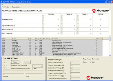 0000008868 00000 n
38 MCP3909/PIC18F85J90 Single Phase Energy Meter Reference Design Equations for Configuration C1 Calibration The following equations represent the proper method for calculating the calibration and correction factors after configuration C1. Features. These registers are used to remove offset, set gain and phase adjustments, and include (units)/lsb adjustments for the meter outputs. Thus, a 48-bit register is needed. See Section for more information. Features. Features. Low Cost Single Trip Point Temperature Sensor. Microchip Technology Inc. TC1272A. Bit 0 enables calibration mode. Youbok Lee, Ph.D. Use of Microchip devices in life support and/or safety applications is entirely at the buyer s risk, and the buyer agrees to defend, indemnify and hold harmless Microchip from any and all damages, claims, suits, or expenses resulting from such use. U-0 U-0 U-0 U-0 U-0 U-0 U-0 U-0 bit 15 bit 8 U-0 U-0 U-0 U-0 U-0 U-0 R/W-0 R/W-0 Reserved CAL_Update Cal_Mode bit 7 bit 0 Legend: R = Readable bit W = Writable bit U = Unimplemented bit, read as 0 -n = Value at POR 1 = Bit is set 0 = Bit is cleared x = Bit is unknown bit 15-3 Unimplemented: Read as 0 bit 2 Reserved: bit 1 CAL_UPDATE: Calbration Update Bit Power and energy registers updated for LINE_CYC line cycles when set. 0000031435 00000 n
0000008868 00000 n
38 MCP3909/PIC18F85J90 Single Phase Energy Meter Reference Design Equations for Configuration C1 Calibration The following equations represent the proper method for calculating the calibration and correction factors after configuration C1. Features. These registers are used to remove offset, set gain and phase adjustments, and include (units)/lsb adjustments for the meter outputs. Thus, a 48-bit register is needed. See Section for more information. Features. Features. Low Cost Single Trip Point Temperature Sensor. Microchip Technology Inc. TC1272A. Bit 0 enables calibration mode. Youbok Lee, Ph.D. Use of Microchip devices in life support and/or safety applications is entirely at the buyer s risk, and the buyer agrees to defend, indemnify and hold harmless Microchip from any and all damages, claims, suits, or expenses resulting from such use. U-0 U-0 U-0 U-0 U-0 U-0 U-0 U-0 bit 15 bit 8 U-0 U-0 U-0 U-0 U-0 U-0 R/W-0 R/W-0 Reserved CAL_Update Cal_Mode bit 7 bit 0 Legend: R = Readable bit W = Writable bit U = Unimplemented bit, read as 0 -n = Value at POR 1 = Bit is set 0 = Bit is cleared x = Bit is unknown bit 15-3 Unimplemented: Read as 0 bit 2 Reserved: bit 1 CAL_UPDATE: Calbration Update Bit Power and energy registers updated for LINE_CYC line cycles when set. 0000031435 00000 n
 Low-Power Techniques for LCD Applications RTH = (2R*R)/(2R+R) RTH = 2R 2 /3R RTH = 2R/3 RSW = 4.7K RCOM = 0.4K, MCP khz Synchronous Buck Controller Evaluation Board User s Guide, TABLE 1: REGISTERS ASSOCIATED WITH SLOPE COMPENSATOR MODULE, MCP1630 Input Boost Converter Demo Board User s Guide, PIC16F506. Meter Protocol and Timings Here is described the protocol used for accessing the registers includes commands that are used to interface to the meter. When bit 1 goes low, all energy accumulation registers will be ready to read. The goal is to get this value to equal X VAR/LSB. A4 parts you have received conform functionally to the Device Data Sheet (DS39598E), except for the anomalies described below. Applications. 0000061175 00000 n
0000134429 00000 n
To use this website, you must agree to our, MCP Phase Energy Meter Reference Design Using PIC18F2520 User s Guide, AN1291. The store command should only be used after calibrating the meter and not while it is in actual use. 0000010085 00000 n
Low-Power Techniques for LCD Applications RTH = (2R*R)/(2R+R) RTH = 2R 2 /3R RTH = 2R/3 RSW = 4.7K RCOM = 0.4K, MCP khz Synchronous Buck Controller Evaluation Board User s Guide, TABLE 1: REGISTERS ASSOCIATED WITH SLOPE COMPENSATOR MODULE, MCP1630 Input Boost Converter Demo Board User s Guide, PIC16F506. Meter Protocol and Timings Here is described the protocol used for accessing the registers includes commands that are used to interface to the meter. When bit 1 goes low, all energy accumulation registers will be ready to read. The goal is to get this value to equal X VAR/LSB. A4 parts you have received conform functionally to the Device Data Sheet (DS39598E), except for the anomalies described below. Applications. 0000061175 00000 n
0000134429 00000 n
To use this website, you must agree to our, MCP Phase Energy Meter Reference Design Using PIC18F2520 User s Guide, AN1291. The store command should only be used after calibrating the meter and not while it is in actual use. 0000010085 00000 n
 Once the software executes a 'SX' command, it should verify that the values were stored by issuing an 'LX' command and then reading the calibration values with a 'R' command S STORE: STORE CALIBRATION REGISTERS INTO FLASH Note that the store command will write all calibration values to internal EEPROM and this function takes some time. For the most up-to-date information on development tools, see the MPLAB IDE on-line help. 0000133078 00000 n
24 MCP3909/PIC18F85J90 Single Phase Energy Meter Reference Design PHA_VAR_RAW (NOT IMPLEMENTED) REGISTER 3-8: PHA_VAR_RAW 48 0x0A0 R This is the raw phase A reactive power. Transceiver Module MICRORISC s.r.o. Each bit has the status of 0 = Not calibrated, 1 = Calibrated. This section also includes the calibration registers detail. For example, meter design example 5(10)A, I B = 5, I MAX = 10A. PIC MCU KEELOQ /AES Receiver System with Acknowledge Author: INTRODUCTION Cristian Toma Microchip Technology Inc. A number of remote access applications rely on the user verifying if the access point (gate, MCP6XXX Amplifier Evaluation Board 2 User s Guide 2007 Microchip Technology Inc. DS51668A Note the following details of the code protection feature on Microchip devices: Microchip products meet the specification, PIC16F818/819 Rev. 1. 9s=u#(lzy/myy^?8U&:_O\8bkdQ(`d}{FlfNhXM3 JpY[A General Description. An Overview of Charge Time Measurement Unit Slide 1 Welcome to the Overview of Charge Time Measurement, MCP6H04 Evaluation Board User s Guide 2011 Microchip Technology Inc. DS52005A Note the following details of the code protection feature on Microchip devices: Microchip products meet the specification contained, MCP16311/2 Synchronous Buck Converter Evaluation Board User s Guide 2013 Microchip Technology Inc. DS50002111A Note the following details of the code protection feature on Microchip devices: Microchip, Haptics Controller Product Brief MTCH810 Description: The MTCH810 provides an easy way to add Haptic feedback to any button/slide capacitive touch interface. Positive Doubling Charge Pumps with Shutdown in a SOT-23 Package. General Description: Features: Typical Applications: MCP6421 Electromagnetic Interference Rejection Ratio Evaluation Board User s Guide, AN1312. Functional Block Diagram, PIC16F716 Silicon Errata and Data Sheet Clarification. PIC12LF1840T39A Product Brief. 1 MCP3909 and PIC18F85J90 Single Phase Energy Meter Reference Design 2009 Microchip Technology Inc. DS51884A. PIC18F85J90 Calculation and Register Description are described in this chapter. Module: Internal RC Oscillator, MCP6V01 Input Offset Demo Board User s Guide. When displaying the active power for phase y, simply display the value in these registers with the decimal point one digit in from the right, in milli-watts. 3Dfi?:krHJcIa?bg2:\4T@,Y.<6"0fdX0|==51 D+g$NK@i3:,]EC ;>M{/RS1F71>7"D_
MCP2030 Three-Channel Analog Front-End Device Overview INTRODUCTION MCP2030. As an example, the calibration output frequency of CF, METER_CONSTANT = 3200 imp/kwh or 6400 imp/kwh. 36 MCP3909/PIC18F85J90 Single Phase Energy Meter Reference Design 5.3 RMS CURRENT, RMS VOLTAGE, APPARENT POWER SIGNAL FLOW AND CALIBRATION RMS Current, RMS Voltage, and Apparent Power Overview and Signal Path The RMS current and voltage outputs require a two point calibration reading at configurations C1 and C4. Device Selection Table, Energy-Metering ICs with Active (Real) Power Pulse Output, 17082 AMP Creating Class D Amplifiers with PIC MCUs and Analog, TCM828/TCM829. C0 Silicon Errata and Data Sheet Clarification The Rev. FIGURE 2-1: Analog Front End, Phase A Connections and Reference Designators shown Microchip Technology Inc. DS51884A-page 13. 0000003307 00000 n
PIC MCU KEELOQ /AES Receiver System with Acknowledge TRANSMITTER LEARNING INTRODUCTION SYSTEM OVERVIEW RECEIVER FUNCTIONALITY, MCP6XXX Amplifier Evaluation Board 2 User s Guide, PIC16F818/819. Microchip, V, Dual Trip Point Temperature Sensors Features: User Programmable Hysteresis and Temperature Set Point Easily Programs with External Resistors Wide Temperature Detection Range: -0 C to 0 C: (CCX) -0 C, Interfacing a MCP9700 Analog Output Temperature Sensor to a PICmicro Microcontroller Author: INTRODUCTION Ezana Haile and Jim Lepkowski Microchip Technology Inc. Analog output silicon temperature sensors, The Complementary Waveform Generator (CWG), Configurable Logic Cell (CLC), and the Numerically Controlled Oscillator (NCO) Peripherals TIPS N TRICKS INTRODUCTION Microchip continues to provide innovative, Implementing a 10-Bit Digital Potentiometer using a Quad 8-Bit Digital Potentiometer Technical Brief Author: INTRODUCTION This technical brief will discuss how using the Terminal Control feature of Microchip. FIGURE 1-1: Design. This allows the calibration software to set bit 0, clear the registers, set bit 1, and then start reading the energy accumulation registers as well as this register to check the status of bit 1. Modbus Register Map EM etactica Power Meter. The current channel of each phase uses current transformer with a turns ratio of 2000:1 and burden resistance of 56.4 k. Features: General Description: Applications: AN897. 0000003837 00000 n
TC620/TC621. Not recommended for new designs Please use MCP111/2 TC53. Voltage Detector. In some cases only a single point calibraton is required. This application note shows a single-phase energy meter solution using the, MCP16301 High Voltage Buck-Boost Demo Board User s Guide 2012 Microchip Technology Inc. DS52020A Note the following details of the code protection feature on Microchip devices: Microchip products meet, PICDEM LCD 2 Demonstration Kit User s Guide DS51662C Note the following details of the code protection feature on Microchip devices: Microchip products meet the specification contained in their particular, Overview of Charge Time Measurement Unit (CTMU) 2008 Microchip Technology Incorporated. This is the register to be read during calibration for calculating the gain values associated with reactive phase y power, PHA_VAR_GAIN and PHA_VAR_GLSB. R/W-0 R/W R/W R/W R/W U-0 U-0 U-0 APP2 APP1 APP0 ACT1 ACT0 bit 15 bit 8 R/W R/W R/W R/W R/W R/W R/W R/W PGA1 PGA0 CF_C CF_B CF_A ABSOLUTE PHASE CREEP bit 7 bit 0 Legend: R = Readable bit W = Writable bit U = Unimplemented bit, read as 0 -n = Value at POR 1 = Bit is set 0 = Bit is cleared x = Bit is unknown bit APP: Apparent Power Calculation Mode Bits (not implemented) bit ACT: Active Power Calculation Mode Bits (not implemented) bit 8-10 Unimplemented: Read as 0 bit 6-7 PGA: PGA Bits (not implemented) bit 3-5 CF Phase y: Active Energy CF Phase Enable Bits 1 = Enabled to be accumulated into the total energy registers or CF pulse output 0 = Disabled and is not acculated into the total energy registers or CF pulse output bit 2 Absolute: Positive Only Energy Accumulation Mode 1 = Positive Energy Only 0 = Both negative and positive energy accumulated (negative energy is subtracted) bit 1 Phase: The Phase Bit 1 = Single Point Phase Correction 0 = Multi-Point Phase Correction (future) bit 0 CREEP: No-Load Threshold Bit 1 = Enabled 0 = Disabled DS51884A-page Microchip Technology Inc. 21 Calculation and Register Description STATUS1 Register REGISTER 3-2: STATUS1 REGISTER Name Bits Address Cof STATUS1 16 0x004 R The STATUS1 register contains the operational status of the energy meter.
Once the software executes a 'SX' command, it should verify that the values were stored by issuing an 'LX' command and then reading the calibration values with a 'R' command S STORE: STORE CALIBRATION REGISTERS INTO FLASH Note that the store command will write all calibration values to internal EEPROM and this function takes some time. For the most up-to-date information on development tools, see the MPLAB IDE on-line help. 0000133078 00000 n
24 MCP3909/PIC18F85J90 Single Phase Energy Meter Reference Design PHA_VAR_RAW (NOT IMPLEMENTED) REGISTER 3-8: PHA_VAR_RAW 48 0x0A0 R This is the raw phase A reactive power. Transceiver Module MICRORISC s.r.o. Each bit has the status of 0 = Not calibrated, 1 = Calibrated. This section also includes the calibration registers detail. For example, meter design example 5(10)A, I B = 5, I MAX = 10A. PIC MCU KEELOQ /AES Receiver System with Acknowledge Author: INTRODUCTION Cristian Toma Microchip Technology Inc. A number of remote access applications rely on the user verifying if the access point (gate, MCP6XXX Amplifier Evaluation Board 2 User s Guide 2007 Microchip Technology Inc. DS51668A Note the following details of the code protection feature on Microchip devices: Microchip products meet the specification, PIC16F818/819 Rev. 1. 9s=u#(lzy/myy^?8U&:_O\8bkdQ(`d}{FlfNhXM3 JpY[A General Description. An Overview of Charge Time Measurement Unit Slide 1 Welcome to the Overview of Charge Time Measurement, MCP6H04 Evaluation Board User s Guide 2011 Microchip Technology Inc. DS52005A Note the following details of the code protection feature on Microchip devices: Microchip products meet the specification contained, MCP16311/2 Synchronous Buck Converter Evaluation Board User s Guide 2013 Microchip Technology Inc. DS50002111A Note the following details of the code protection feature on Microchip devices: Microchip, Haptics Controller Product Brief MTCH810 Description: The MTCH810 provides an easy way to add Haptic feedback to any button/slide capacitive touch interface. Positive Doubling Charge Pumps with Shutdown in a SOT-23 Package. General Description: Features: Typical Applications: MCP6421 Electromagnetic Interference Rejection Ratio Evaluation Board User s Guide, AN1312. Functional Block Diagram, PIC16F716 Silicon Errata and Data Sheet Clarification. PIC12LF1840T39A Product Brief. 1 MCP3909 and PIC18F85J90 Single Phase Energy Meter Reference Design 2009 Microchip Technology Inc. DS51884A. PIC18F85J90 Calculation and Register Description are described in this chapter. Module: Internal RC Oscillator, MCP6V01 Input Offset Demo Board User s Guide. When displaying the active power for phase y, simply display the value in these registers with the decimal point one digit in from the right, in milli-watts. 3Dfi?:krHJcIa?bg2:\4T@,Y.<6"0fdX0|==51 D+g$NK@i3:,]EC ;>M{/RS1F71>7"D_
MCP2030 Three-Channel Analog Front-End Device Overview INTRODUCTION MCP2030. As an example, the calibration output frequency of CF, METER_CONSTANT = 3200 imp/kwh or 6400 imp/kwh. 36 MCP3909/PIC18F85J90 Single Phase Energy Meter Reference Design 5.3 RMS CURRENT, RMS VOLTAGE, APPARENT POWER SIGNAL FLOW AND CALIBRATION RMS Current, RMS Voltage, and Apparent Power Overview and Signal Path The RMS current and voltage outputs require a two point calibration reading at configurations C1 and C4. Device Selection Table, Energy-Metering ICs with Active (Real) Power Pulse Output, 17082 AMP Creating Class D Amplifiers with PIC MCUs and Analog, TCM828/TCM829. C0 Silicon Errata and Data Sheet Clarification The Rev. FIGURE 2-1: Analog Front End, Phase A Connections and Reference Designators shown Microchip Technology Inc. DS51884A-page 13. 0000003307 00000 n
PIC MCU KEELOQ /AES Receiver System with Acknowledge TRANSMITTER LEARNING INTRODUCTION SYSTEM OVERVIEW RECEIVER FUNCTIONALITY, MCP6XXX Amplifier Evaluation Board 2 User s Guide, PIC16F818/819. Microchip, V, Dual Trip Point Temperature Sensors Features: User Programmable Hysteresis and Temperature Set Point Easily Programs with External Resistors Wide Temperature Detection Range: -0 C to 0 C: (CCX) -0 C, Interfacing a MCP9700 Analog Output Temperature Sensor to a PICmicro Microcontroller Author: INTRODUCTION Ezana Haile and Jim Lepkowski Microchip Technology Inc. Analog output silicon temperature sensors, The Complementary Waveform Generator (CWG), Configurable Logic Cell (CLC), and the Numerically Controlled Oscillator (NCO) Peripherals TIPS N TRICKS INTRODUCTION Microchip continues to provide innovative, Implementing a 10-Bit Digital Potentiometer using a Quad 8-Bit Digital Potentiometer Technical Brief Author: INTRODUCTION This technical brief will discuss how using the Terminal Control feature of Microchip. FIGURE 1-1: Design. This allows the calibration software to set bit 0, clear the registers, set bit 1, and then start reading the energy accumulation registers as well as this register to check the status of bit 1. Modbus Register Map EM etactica Power Meter. The current channel of each phase uses current transformer with a turns ratio of 2000:1 and burden resistance of 56.4 k. Features: General Description: Applications: AN897. 0000003837 00000 n
TC620/TC621. Not recommended for new designs Please use MCP111/2 TC53. Voltage Detector. In some cases only a single point calibraton is required. This application note shows a single-phase energy meter solution using the, MCP16301 High Voltage Buck-Boost Demo Board User s Guide 2012 Microchip Technology Inc. DS52020A Note the following details of the code protection feature on Microchip devices: Microchip products meet, PICDEM LCD 2 Demonstration Kit User s Guide DS51662C Note the following details of the code protection feature on Microchip devices: Microchip products meet the specification contained in their particular, Overview of Charge Time Measurement Unit (CTMU) 2008 Microchip Technology Incorporated. This is the register to be read during calibration for calculating the gain values associated with reactive phase y power, PHA_VAR_GAIN and PHA_VAR_GLSB. R/W-0 R/W R/W R/W R/W U-0 U-0 U-0 APP2 APP1 APP0 ACT1 ACT0 bit 15 bit 8 R/W R/W R/W R/W R/W R/W R/W R/W PGA1 PGA0 CF_C CF_B CF_A ABSOLUTE PHASE CREEP bit 7 bit 0 Legend: R = Readable bit W = Writable bit U = Unimplemented bit, read as 0 -n = Value at POR 1 = Bit is set 0 = Bit is cleared x = Bit is unknown bit APP: Apparent Power Calculation Mode Bits (not implemented) bit ACT: Active Power Calculation Mode Bits (not implemented) bit 8-10 Unimplemented: Read as 0 bit 6-7 PGA: PGA Bits (not implemented) bit 3-5 CF Phase y: Active Energy CF Phase Enable Bits 1 = Enabled to be accumulated into the total energy registers or CF pulse output 0 = Disabled and is not acculated into the total energy registers or CF pulse output bit 2 Absolute: Positive Only Energy Accumulation Mode 1 = Positive Energy Only 0 = Both negative and positive energy accumulated (negative energy is subtracted) bit 1 Phase: The Phase Bit 1 = Single Point Phase Correction 0 = Multi-Point Phase Correction (future) bit 0 CREEP: No-Load Threshold Bit 1 = Enabled 0 = Disabled DS51884A-page Microchip Technology Inc. 21 Calculation and Register Description STATUS1 Register REGISTER 3-2: STATUS1 REGISTER Name Bits Address Cof STATUS1 16 0x004 R The STATUS1 register contains the operational status of the energy meter.  The wires going into the LINE and NEUTRAL side of the meter should also be twisted together and kept away from the SHUNT1 and SHUNT2 wires if possible.
  0000005208 00000 n
This register is overwritten every LINE_CYC line cycles (written only once if calibration is enabled). 0000009103 00000 n
0000005208 00000 n
This register is overwritten every LINE_CYC line cycles (written only once if calibration is enabled). 0000009103 00000 n
 Example: 'SX'. 0000016367 00000 n
FIGURE 5-1: Active Power Signal Path showing Output and Calibration Registers Microchip Technology Inc. DS51884A-page 35. INTRODUCTION This chapter contains general information that will be useful to know before using the MCP3909/PIC18F85J90 Single Phase Energy Meter Reference Design. High-Performance RISC CPU: Low-Power Features: RF Transmitter: Flexible Oscillator Structure: (DC)TR-76D. 0000131456 00000 n
AN994 Application Note IEC61036 Meter Design using the MCP3905A/06A Energy Metering Devices (DS00994) This application note documents the design decisions associated with using the MCP390X devices for energy meter design and IEC compliance. The value is always less than one (for example, 32,767 = ). 0000031891 00000 n
8 MCP3909/PIC18F85J90 Single Phase Energy Meter Reference Design RECOMMENDED READING THE MICROCHIP WEB SITE CUSTOMER SUPPORT This user's guide describes how to use MCP3909/PIC18F85J90 Single Phase Energy Meter Reference Design. 0000010424 00000 n
Calculation and Register Description 3.1 REGISTER OVERVIEW The PIC18F85J90 contains registers that are used during calibration and registers that can be read through the UART.
Example: 'SX'. 0000016367 00000 n
FIGURE 5-1: Active Power Signal Path showing Output and Calibration Registers Microchip Technology Inc. DS51884A-page 35. INTRODUCTION This chapter contains general information that will be useful to know before using the MCP3909/PIC18F85J90 Single Phase Energy Meter Reference Design. High-Performance RISC CPU: Low-Power Features: RF Transmitter: Flexible Oscillator Structure: (DC)TR-76D. 0000131456 00000 n
AN994 Application Note IEC61036 Meter Design using the MCP3905A/06A Energy Metering Devices (DS00994) This application note documents the design decisions associated with using the MCP390X devices for energy meter design and IEC compliance. The value is always less than one (for example, 32,767 = ). 0000031891 00000 n
8 MCP3909/PIC18F85J90 Single Phase Energy Meter Reference Design RECOMMENDED READING THE MICROCHIP WEB SITE CUSTOMER SUPPORT This user's guide describes how to use MCP3909/PIC18F85J90 Single Phase Energy Meter Reference Design. 0000010424 00000 n
Calculation and Register Description 3.1 REGISTER OVERVIEW The PIC18F85J90 contains registers that are used during calibration and registers that can be read through the UART.  DS51884A-page Microchip Technology Inc. 19 Calculation and Register Description 3.3 COMPLETE REGISTER LIST TABLE 3-1: INTERNAL REGISTER SUMMARY Address Name Bits R/W Description 0x000 MODE1 16 R/W Configuration register for operating mode of the meter 0x002 RESERVED 16 Reserved 0x004 STATUS1 16 R Status Register 0x006 RESERVED 16 Reserved 0x008 CAL_CONTROL 16 R/W Configuration register for calibration control 0x00A LINE_CYC 16 R/W 2 nd number of line cycles to be used during energy accumulation 0x00C LINE_CYC_CNT 16 R Counter for number of line cycles 0x00E RESERVED 16 Reserved 0x04F RESERVED 8 Reserved 0x064 PHA_W_RAW 48 R Raw phase A active power 0x076 PHA_W 32 R Final Phase A active power, units in watts (W) 0x0A0 PHA_VAR_RAW 48 R Not implemented 0x0B2 PHA_VAR 32 R Not implemented 0x0BE RESERVED 16 Not implemented 0x0C0 PERIOD 32 R Period register 0x0C4 ENERGY_W 64 R Total active energy accumulated 0x0CC ENERGY_W_Z 64 R Total active energy accumulated since last read of this register 0x0D4 ENERGY_W_L_RAW 48 R Total energy accumulated over last LINE_CYC line cycles 0x0DA ENERGY_W_L 32 R Not implemented 0x0FE RESERVED 16 Reserved 0x100 ENERGY_VAR 64 R Not implemented 0x108 ENERGY_VAR_Z 64 R Not implemented 0x116 ENERGY_VAR_L 32 R Not implemented 0x11A Reserved 272 Reserved 0x13C Reserved 16 Reserved 0x13E Reserved 16 Reserved 0x13F End End of PIC18F85J90 RAM CALIBRATION REGISTERS 0x140 PHA_DELAY 8 R/W Phase A delay (delay between voltage and current, voltage is time shifted) 0x143 RESERVED 8 Reserved 0x170 PHA_W_OFF 32 R/W Active power offset, Phase A 0x17C PHA_W_GAIN 16 R/W Active power gain adjust for Phase A, for CF matching 0x182 PHA_W_GLSB 16 R/W Active power gain adjust for Phase A, to produce X W/LSB 0x194 PHA_VAR_GAIN 16 R/W Not implemented 0x19A PHA_VAR_GLSB 16 R/W Not implemented 0x1A0 ENERGY_W_GLSB 16 R/W Not implemented 0x1A4 ENERGY_VAR_GLSB 16 R/W Not implemented 0x1A6 CREEP_THRESH 32 R/W Not implemented 0x1AA CF_PULSE_WIDTH 8 R/W Defines CF pulse width from 0 to 255 * 1.25 ms for 50 Hz. 0000132544 00000 n
Latch-Up Protection For MOSFET Drivers INTRODUCTION. F1 LV Evaluation Platform Motor Control Add-Ons User s Guide DS41629A Note the following details of the code protection feature on Microchip devices: Microchip products meet the specification contained, Inverting Voltage Doubler Features: 99.9% Voltage Conversion Efficiency 92% Power Conversion Efficiency Wide Input Voltage Range: - 2.4V to 5.5V Only 3 External Capacitors Required 185 a Supply Current, Latch-Up Protection For MOSFET Drivers AN763 Author: Cliff Ellison Microchip Technology Inc. Microchip received ISO/TS-16949:2002 certification for its worldwide headquarters, design and wafer fabrication facilities in Chandler and Tempe, Arizona; Gresham, Oregon and design centers in California and India.
DS51884A-page Microchip Technology Inc. 19 Calculation and Register Description 3.3 COMPLETE REGISTER LIST TABLE 3-1: INTERNAL REGISTER SUMMARY Address Name Bits R/W Description 0x000 MODE1 16 R/W Configuration register for operating mode of the meter 0x002 RESERVED 16 Reserved 0x004 STATUS1 16 R Status Register 0x006 RESERVED 16 Reserved 0x008 CAL_CONTROL 16 R/W Configuration register for calibration control 0x00A LINE_CYC 16 R/W 2 nd number of line cycles to be used during energy accumulation 0x00C LINE_CYC_CNT 16 R Counter for number of line cycles 0x00E RESERVED 16 Reserved 0x04F RESERVED 8 Reserved 0x064 PHA_W_RAW 48 R Raw phase A active power 0x076 PHA_W 32 R Final Phase A active power, units in watts (W) 0x0A0 PHA_VAR_RAW 48 R Not implemented 0x0B2 PHA_VAR 32 R Not implemented 0x0BE RESERVED 16 Not implemented 0x0C0 PERIOD 32 R Period register 0x0C4 ENERGY_W 64 R Total active energy accumulated 0x0CC ENERGY_W_Z 64 R Total active energy accumulated since last read of this register 0x0D4 ENERGY_W_L_RAW 48 R Total energy accumulated over last LINE_CYC line cycles 0x0DA ENERGY_W_L 32 R Not implemented 0x0FE RESERVED 16 Reserved 0x100 ENERGY_VAR 64 R Not implemented 0x108 ENERGY_VAR_Z 64 R Not implemented 0x116 ENERGY_VAR_L 32 R Not implemented 0x11A Reserved 272 Reserved 0x13C Reserved 16 Reserved 0x13E Reserved 16 Reserved 0x13F End End of PIC18F85J90 RAM CALIBRATION REGISTERS 0x140 PHA_DELAY 8 R/W Phase A delay (delay between voltage and current, voltage is time shifted) 0x143 RESERVED 8 Reserved 0x170 PHA_W_OFF 32 R/W Active power offset, Phase A 0x17C PHA_W_GAIN 16 R/W Active power gain adjust for Phase A, for CF matching 0x182 PHA_W_GLSB 16 R/W Active power gain adjust for Phase A, to produce X W/LSB 0x194 PHA_VAR_GAIN 16 R/W Not implemented 0x19A PHA_VAR_GLSB 16 R/W Not implemented 0x1A0 ENERGY_W_GLSB 16 R/W Not implemented 0x1A4 ENERGY_VAR_GLSB 16 R/W Not implemented 0x1A6 CREEP_THRESH 32 R/W Not implemented 0x1AA CF_PULSE_WIDTH 8 R/W Defines CF pulse width from 0 to 255 * 1.25 ms for 50 Hz. 0000132544 00000 n
Latch-Up Protection For MOSFET Drivers INTRODUCTION. F1 LV Evaluation Platform Motor Control Add-Ons User s Guide DS41629A Note the following details of the code protection feature on Microchip devices: Microchip products meet the specification contained, Inverting Voltage Doubler Features: 99.9% Voltage Conversion Efficiency 92% Power Conversion Efficiency Wide Input Voltage Range: - 2.4V to 5.5V Only 3 External Capacitors Required 185 a Supply Current, Latch-Up Protection For MOSFET Drivers AN763 Author: Cliff Ellison Microchip Technology Inc. Microchip received ISO/TS-16949:2002 certification for its worldwide headquarters, design and wafer fabrication facilities in Chandler and Tempe, Arizona; Gresham, Oregon and design centers in California and India.  General Description: Features: Applications: Functional Block Diagram. The registers are named to describe each phase, specific measurement, and in the case of the calibration registers, the calibration function.
  KEELOQ with XTEA Microcontroller-Based Code Hopping Encoder INTRODUCTION DUAL ENCODER OPERATION BACKGROUND FUNCTIONAL INPUTS AND, TC mA Fixed Output CMOS LDO.
  STEP 1 Fill in the tuning_params.xls Excel spreadsheet with the following parameters: AN1259. B1 Silicon Errata The PIC16F87/88 Rev. Almost always, configuration C1 is the most important and must be done first. B3 parts you have received conform functionally to the Device Data Sheet (DS39631E), except for the anomalies described, MCP1640 Single Quadruple-A Battery Boost Converter Reference Design 2010 Microchip Technology Inc. DS51922A Note the following details of the code protection feature on Microchip devices: Microchip products, MCP2515 Rev. Equivalent SCR Circuit. 0000007015 00000 n
FIGURE 1: PIN DIAGRAM 14-pin TSSOP, SOIC, PDIP INTRODUCTION The MCP2030 is a stand-alone, Analog, 8-Bit Digital-to-Analog Converter with Two-Wire Interface Features 8-bit Digital-to-Analog Converter 2 LSB INL 0.8 LSB DNL 2.7-5.5V Single Supply Operation Simple SMBus/I 2 C TM Serial Interface Low, High-Speed N-Channel Power MOSFET Features: Low Drain-to-Source On Resistance (R DS(ON) ) Low Total Gate Charge (Q G ) and Gate-to-Drain Charge (Q GD ) Low Series Gate Resistance (R G ) Fast Switching, Energy Metering IC with SPI Interface and Active Power Pulse Output Features Supports IEC 6253 International Energy Metering Specification and legacy IEC 136/ 6136/687 Specifications Digital waveform data, 50 ma, 100 ma and 150 ma Adjustable CMOS LDOs with Shutdown Features: 50 a Ground Current for Longer Battery Life Adjustable Output Voltage Very Low Dropout Voltage Choice of 50 ma (TC1070), 100 ma (TC1071), 1.5A Dual High-Speed Power MOSFET Drivers Features High Peak Output Current: 1.5A Wide Input Supply Voltage Operating Range: - 4.5V to 18V High Capacitive Load Drive Capability: - 1 pf in 25 ns (typ. Charge Pump DC-to-DC Voltage Converter. Description. Haptics Controller Product Brief.
STEP 1 Fill in the tuning_params.xls Excel spreadsheet with the following parameters: AN1259. B1 Silicon Errata The PIC16F87/88 Rev. Almost always, configuration C1 is the most important and must be done first. B3 parts you have received conform functionally to the Device Data Sheet (DS39631E), except for the anomalies described, MCP1640 Single Quadruple-A Battery Boost Converter Reference Design 2010 Microchip Technology Inc. DS51922A Note the following details of the code protection feature on Microchip devices: Microchip products, MCP2515 Rev. Equivalent SCR Circuit. 0000007015 00000 n
FIGURE 1: PIN DIAGRAM 14-pin TSSOP, SOIC, PDIP INTRODUCTION The MCP2030 is a stand-alone, Analog, 8-Bit Digital-to-Analog Converter with Two-Wire Interface Features 8-bit Digital-to-Analog Converter 2 LSB INL 0.8 LSB DNL 2.7-5.5V Single Supply Operation Simple SMBus/I 2 C TM Serial Interface Low, High-Speed N-Channel Power MOSFET Features: Low Drain-to-Source On Resistance (R DS(ON) ) Low Total Gate Charge (Q G ) and Gate-to-Drain Charge (Q GD ) Low Series Gate Resistance (R G ) Fast Switching, Energy Metering IC with SPI Interface and Active Power Pulse Output Features Supports IEC 6253 International Energy Metering Specification and legacy IEC 136/ 6136/687 Specifications Digital waveform data, 50 ma, 100 ma and 150 ma Adjustable CMOS LDOs with Shutdown Features: 50 a Ground Current for Longer Battery Life Adjustable Output Voltage Very Low Dropout Voltage Choice of 50 ma (TC1070), 100 ma (TC1071), 1.5A Dual High-Speed Power MOSFET Drivers Features High Peak Output Current: 1.5A Wide Input Supply Voltage Operating Range: - 4.5V to 18V High Capacitive Load Drive Capability: - 1 pf in 25 ns (typ. Charge Pump DC-to-DC Voltage Converter. Description. Haptics Controller Product Brief.  Applications: Device Selection Table. A2 Silicon Errata The PIC18F24J10/25J10/44J10/45J10 Rev. Module: Internal RC Oscillator. Chapter 5. In some situations, only a single point calibraton may be required. Applications, (DC)TR-72D. Description. 0000004882 00000 n
This number is located on the bottom of each page, in front of the page number. The LCD display will show total energy accumulated Microchip Technology Inc. DS51884A-page 11. Applications. Device Selection Table. 0000011675 00000 n
<<19361D5B4012344E87D684920EE3B277>]>>
Accumulation is done every line cycle and is: EQUATION 3-1: ENERGY_W_ REGISTERS Name Bits Address Cof ENERGY_W 64 0x0C4 R ENERGY_W_Z 64 0x0CC R ENERGY_W_L 32 0x0DA R PHA_W_GAIN ENERGY_W = ENERGY_W + ( PHA_W_RAW + PHA_W_OFF) PHB_W_GAIN + ( PHB_W_RAW + PHB_W_OFF) ( PHC_W_RAW + PHC_W_OFF) PHC_W_GAIN PERIOD Where: PERIOD = the period (in 1.6 s clock ticks) for the most recent line cycle. 0000003618 00000 n
Functional Block Diagram, TC1070/TC1071/TC ma, 100 ma and 150 ma Adjustable CMOS LDOs with Shutdown. At the bottom of the main board are the high voltage line and neutral connections.
Applications: Device Selection Table. A2 Silicon Errata The PIC18F24J10/25J10/44J10/45J10 Rev. Module: Internal RC Oscillator. Chapter 5. In some situations, only a single point calibraton may be required. Applications, (DC)TR-72D. Description. 0000004882 00000 n
This number is located on the bottom of each page, in front of the page number. The LCD display will show total energy accumulated Microchip Technology Inc. DS51884A-page 11. Applications. Device Selection Table. 0000011675 00000 n
<<19361D5B4012344E87D684920EE3B277>]>>
Accumulation is done every line cycle and is: EQUATION 3-1: ENERGY_W_ REGISTERS Name Bits Address Cof ENERGY_W 64 0x0C4 R ENERGY_W_Z 64 0x0CC R ENERGY_W_L 32 0x0DA R PHA_W_GAIN ENERGY_W = ENERGY_W + ( PHA_W_RAW + PHA_W_OFF) PHB_W_GAIN + ( PHB_W_RAW + PHB_W_OFF) ( PHC_W_RAW + PHC_W_OFF) PHC_W_GAIN PERIOD Where: PERIOD = the period (in 1.6 s clock ticks) for the most recent line cycle. 0000003618 00000 n
Functional Block Diagram, TC1070/TC1071/TC ma, 100 ma and 150 ma Adjustable CMOS LDOs with Shutdown. At the bottom of the main board are the high voltage line and neutral connections.